- 您现在的位置:买卖IC网 > Sheet目录1998 > ICS844021BGI-01LFT (IDT, Integrated Device Technology Inc)IC CLOCK GEN ETHERNET 8-TSSOP
IDT / ICS LVDS CLOCK GENERATOR
8
ICS844021BGI-01 REV. A NOVEMBER 6, 2012
ICS844021I-01
FEMTOCLOCKS CRYSTAL-TO-LVDS CLOCK GENERATOR
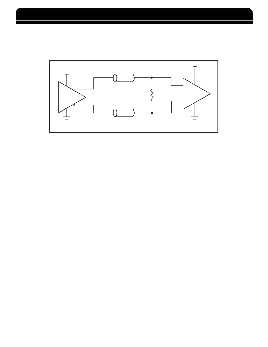
3.3V, 2.5V LVDS DRIVER TERMINATION
A general LVDS interface is shown in
Figure 4 In a 100
Ω
differential transmission line environment, LVDS drivers
require a matched load termination of 100
Ω across near
FIGURE 4. TYPICAL LVDS DRIVER TERMINATION
the receiver input. For a multiple LVDS outputs buffer, if only
partial outputs are used, it is recommended to terminate the
unused outputs.
LVDS Driver
R1
100
Ω
–
+
50
Ω
50
Ω
3.3V or 2.5V
V
DD
100
Ω Differential Transmission Line
发布紧急采购,3分钟左右您将得到回复。
相关PDF资料
ICS844071AGLFT
IC CLOCK GEN GIG ETH 8-TSSOP
ICS844201BG-45LF
IC CLK GENERATOR 25MHZ 8TSSOP
ICS844204BK-245LF
IC CLK SYNTHESIZER 4LVDS 32VFQFN
ICS844S42BKILF
IC SYNTHESIZER RF FREQ 56-VFQFPN
ICS86004BG-01LF
IC CLK BUFFER ZD 1:4 16-TSSOP
ICS8634BY-01LFT
IC BUFFER ZD 1-5 LVPECL 32-LQFP
ICS8701AY-01LF
IC CLK GEN POLARITY CTRL 48-LQFP
ICS8701CYLF
IC CLK GENERATOR /1 /2 48-LQFP
相关代理商/技术参数
ICS8440258AK-46LF
功能描述:IC SYNTHESIZER 8OUTPUT 32-VFQFPN RoHS:是 类别:集成电路 (IC) >> 时钟/计时 - 时钟发生器,PLL,频率合成器 系列:HiPerClockS™, FemtoClock™ 标准包装:1,000 系列:- 类型:时钟/频率合成器,扇出分配 PLL:- 输入:- 输出:- 电路数:- 比率 - 输入:输出:- 差分 - 输入:输出:- 频率 - 最大:- 除法器/乘法器:- 电源电压:- 工作温度:- 安装类型:表面贴装 封装/外壳:56-VFQFN 裸露焊盘 供应商设备封装:56-VFQFP-EP(8x8) 包装:带卷 (TR) 其它名称:844S012AKI-01LFT
ICS8440258AK-46LFT
功能描述:IC SYNTHESIZER 8OUTPUT 32-VFQFPN RoHS:是 类别:集成电路 (IC) >> 时钟/计时 - 时钟发生器,PLL,频率合成器 系列:HiPerClockS™, FemtoClock™ 标准包装:1,000 系列:- 类型:时钟/频率合成器,扇出分配 PLL:- 输入:- 输出:- 电路数:- 比率 - 输入:输出:- 差分 - 输入:输出:- 频率 - 最大:- 除法器/乘法器:- 电源电压:- 工作温度:- 安装类型:表面贴装 封装/外壳:56-VFQFN 裸露焊盘 供应商设备封装:56-VFQFP-EP(8x8) 包装:带卷 (TR) 其它名称:844S012AKI-01LFT
ICS8440258AKI-46LF
功能描述:IC SYNTHESIZER 8OUTPUT 32-VFQFPN RoHS:是 类别:集成电路 (IC) >> 时钟/计时 - 时钟发生器,PLL,频率合成器 系列:HiPerClockS™, FemtoClock™ 标准包装:27 系列:Precision Edge® 类型:频率合成器 PLL:是 输入:PECL,晶体 输出:PECL 电路数:1 比率 - 输入:输出:1:1 差分 - 输入:输出:无/是 频率 - 最大:800MHz 除法器/乘法器:是/无 电源电压:3.135 V ~ 5.25 V 工作温度:0°C ~ 85°C 安装类型:表面贴装 封装/外壳:28-SOIC(0.295",7.50mm 宽) 供应商设备封装:28-SOIC 包装:管件
ICS8440258AKI-46LFT
功能描述:IC SYNTHESIZER 8OUTPUT 32-VFQFPN RoHS:是 类别:集成电路 (IC) >> 时钟/计时 - 时钟发生器,PLL,频率合成器 系列:HiPerClockS™, FemtoClock™ 标准包装:1,000 系列:- 类型:时钟/频率合成器,扇出分配 PLL:- 输入:- 输出:- 电路数:- 比率 - 输入:输出:- 差分 - 输入:输出:- 频率 - 最大:- 除法器/乘法器:- 电源电压:- 工作温度:- 安装类型:表面贴装 封装/外壳:56-VFQFN 裸露焊盘 供应商设备封装:56-VFQFP-EP(8x8) 包装:带卷 (TR) 其它名称:844S012AKI-01LFT
ICS8440259AK-05LF
功能描述:IC SYNTHESIZER 9OUTPUT 32-VFQFPN RoHS:是 类别:集成电路 (IC) >> 时钟/计时 - 时钟发生器,PLL,频率合成器 系列:HiPerClockS™, FemtoClock™ 标准包装:1,000 系列:- 类型:时钟/频率合成器,扇出分配 PLL:- 输入:- 输出:- 电路数:- 比率 - 输入:输出:- 差分 - 输入:输出:- 频率 - 最大:- 除法器/乘法器:- 电源电压:- 工作温度:- 安装类型:表面贴装 封装/外壳:56-VFQFN 裸露焊盘 供应商设备封装:56-VFQFP-EP(8x8) 包装:带卷 (TR) 其它名称:844S012AKI-01LFT
ICS8440259AK-05LFT
功能描述:IC SYNTHESIZER 9OUTPUT 32-VFQFPN RoHS:是 类别:集成电路 (IC) >> 时钟/计时 - 时钟发生器,PLL,频率合成器 系列:HiPerClockS™, FemtoClock™ 标准包装:1,000 系列:- 类型:时钟/频率合成器,扇出分配 PLL:- 输入:- 输出:- 电路数:- 比率 - 输入:输出:- 差分 - 输入:输出:- 频率 - 最大:- 除法器/乘法器:- 电源电压:- 工作温度:- 安装类型:表面贴装 封装/外壳:56-VFQFN 裸露焊盘 供应商设备封装:56-VFQFP-EP(8x8) 包装:带卷 (TR) 其它名称:844S012AKI-01LFT
ICS8440259AK-45LF
功能描述:IC SYNTHESIZER 9OUTPUT 32-VFQFPN RoHS:是 类别:集成电路 (IC) >> 时钟/计时 - 时钟发生器,PLL,频率合成器 系列:HiPerClockS™, FemtoClock™ 标准包装:1,000 系列:- 类型:时钟/频率合成器,扇出分配 PLL:- 输入:- 输出:- 电路数:- 比率 - 输入:输出:- 差分 - 输入:输出:- 频率 - 最大:- 除法器/乘法器:- 电源电压:- 工作温度:- 安装类型:表面贴装 封装/外壳:56-VFQFN 裸露焊盘 供应商设备封装:56-VFQFP-EP(8x8) 包装:带卷 (TR) 其它名称:844S012AKI-01LFT
ICS8440259AK-45LFT
功能描述:IC SYNTHESIZER 9OUTPUT 32-VFQFPN RoHS:是 类别:集成电路 (IC) >> 时钟/计时 - 时钟发生器,PLL,频率合成器 系列:HiPerClockS™, FemtoClock™ 标准包装:1,000 系列:- 类型:时钟/频率合成器,扇出分配 PLL:- 输入:- 输出:- 电路数:- 比率 - 输入:输出:- 差分 - 输入:输出:- 频率 - 最大:- 除法器/乘法器:- 电源电压:- 工作温度:- 安装类型:表面贴装 封装/外壳:56-VFQFN 裸露焊盘 供应商设备封装:56-VFQFP-EP(8x8) 包装:带卷 (TR) 其它名称:844S012AKI-01LFT